Explore Engineers! Let's do it together Engineer Career Work style My Favorites My Values
Explore Engineers! Let's do it together Engineer,Career,Work style My Favorites,My Values
Interview
Explore Engineers!


Office Tour
Explore Engineers' Favorites!


-
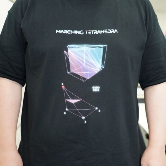
The must-haves "Black T"
I like white T-shirts, but many shoots and experiments in the greenback screen require black costume, so my closed is now full of black T's.
-
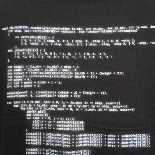
The must-haves "Black T"
However, since a mere black T is boring, I designed it myself to be fashionable. The actual source code is printed in style.
-
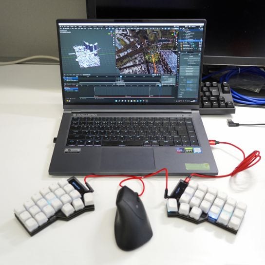
Hand shaped keyboard?
An engineer of content production technology has made his original keyboard with an emphasis on efficiency and functionality. It glows when you tap it.
-
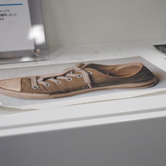
Trick-art
Trick-art uses optical illusions. Engineers of display technology use it to help them think about the principles of vision.
-
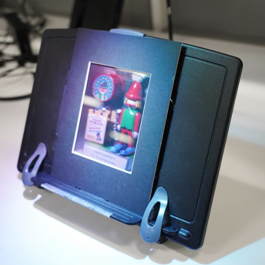
A toy...?
A souvenir from France has been surprisingly the origin of the hologram technology that the display development team is aiming for.
-
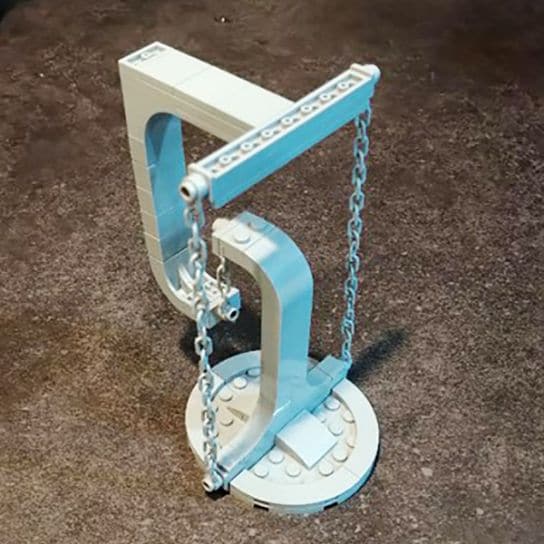
Tensegrity structure block
Sometimes we get ideas from counterintuitive objects or experiences. Tensegrity structures can be mysterious, even though we know the principle in our heads.
-
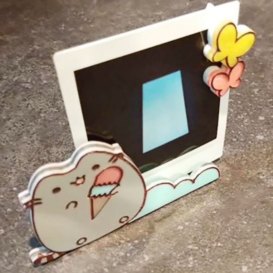
Handmade photo stand
Many people in our company like to make things. Their knowledge of materials and processing methods or their idea inspire me.
-
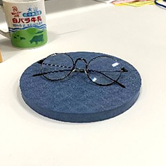
Stretch mat
A mat for kneeling stretches at work. As long as you stretch your hamstring and iliopsoas muscles, you are free from backache.
Explore Working Environment!
-
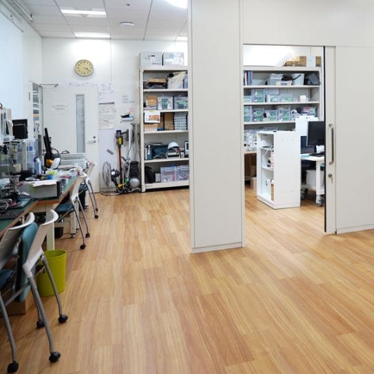
My home?
No, it is the laboratory for the robotics development team. We can move the robots any time in the "fake house", where various types of doors are installed.
-
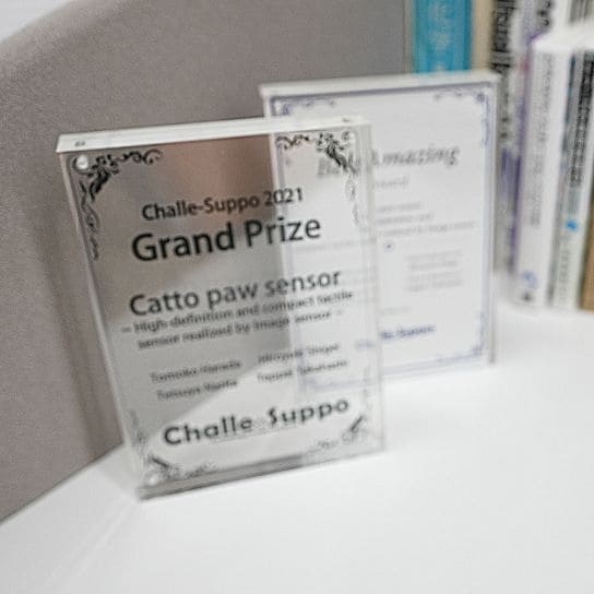
Challe-Suppo Grand Prize plaque!
We've got grand prize of Challe-Suppo, that is the company contest for bottom-up development challenge. It's the result of ideas born from the connection of engineers from different sections! The most favorite point is that all the member's name are engraved on the plaque.
-
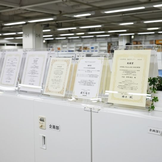
An array of awards certificates!
Many certificates are found all over the office. Every year, company award is given to the outstanding research achievements.
Dive into the clean room!
-
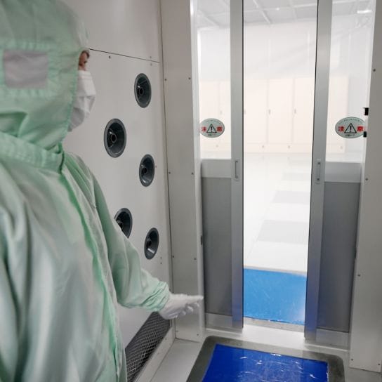
What experiments are you doing here?
Developing light emitting and electronic devices using GaAs, InP, and GaN compound semiconductors, and processing newly developed devices from semiconductor wafers to a state where they can be evaluated.
What phases of development are most often used?
The phase of principle confirmation and characteristic improvement for newly developed devices. Some engineers are here every day.
What is the advantage of Sony's clean room?
A full range of equipment for processing semiconductor wafers to final devices are installed, so we can conduct various studies in a short period of time.
-
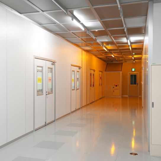
What experiments are you doing here?
Developing light emitting and electronic devices using GaAs, InP, and GaN compound semiconductors, and processing newly developed devices from semiconductor wafers to a state where they can be evaluated.
What phases of development are most often used?
The phase of principle confirmation and characteristic improvement for newly developed devices. Some engineers are here every day.
What is the advantage of Sony's clean room?
A full range of equipment for processing semiconductor wafers to final devices are installed, so we can conduct various studies in a short period of time.
-
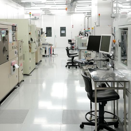
What experiments are you doing here?
Developing light emitting and electronic devices using GaAs, InP, and GaN compound semiconductors, and processing newly developed devices from semiconductor wafers to a state where they can be evaluated.
What phases of development are most often used?
The phase of principle confirmation and characteristic improvement for newly developed devices. Some engineers are here every day.
What is the advantage of Sony's clean room?
A full range of equipment for processing semiconductor wafers to final devices are installed, so we can conduct various studies in a short period of time.
-
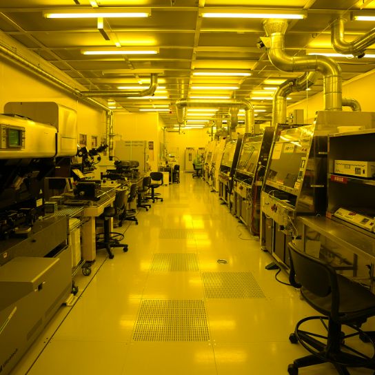
What experiments are you doing here?
Developing light emitting and electronic devices using GaAs, InP, and GaN compound semiconductors, and processing newly developed devices from semiconductor wafers to a state where they can be evaluated.
What phases of development are most often used?
The phase of principle confirmation and characteristic improvement for newly developed devices. Some engineers are here every day.
What is the advantage of Sony's clean room?
A full range of equipment for processing semiconductor wafers to final devices are installed, so we can conduct various studies in a short period of time.


RECRUIT
We are looking for people who want to
promote research and
development of the
worlds most advanced technology and
those
full of motivation to open up the future.

