People
Series: Inside the Minds of Sony’s Corporate Distinguished Engineers #4 Tetsuya Tatsumi
Plasma was, and still is, a key technology for manufacturing
Sep 24, 2021
In this series, Sony’s top engineers discuss their careers, research, and their ideal profile as an engineer at Sony.
In #4, we hear from Tetsuya Tatsumi, who specializes in plasma processing technology.
Corporate Distinguished Engineer
Sony certifies its engineers as "Corporate Distinguished Engineer" who formulate and execute technology strategies while identifying signals of change, and support the development of talent in order to ensure Sony’s sustainable growth.
Profile
-
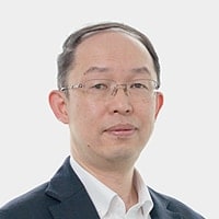
Tetsuya Tatsumi
Distinguished Engineer
Research Div. 2
Sony Semiconductor Solutions
Ph.D. in Engineering
The Japan Society of Applied Physics (JSAP) Fellow
Mesmerized by the beauty and potential of plasma, I made it my life’s work.
Tetsuya Tatsumi was born in the suburb of Tokyo. Since childhood, he has loved music and technology.
When I was in elementary school, my parents bought me a transistor radio, and that sparked my interest in technology. I wasn’t good at mathematics and science, but I like them. I rather preferred art, music, and technical classes.
In high school, I joined the classical guitar club, where there were plenty of opportunities to learn about music and use audio equipment such as tape recorders and record players. At one point, I was also very passionate about BCL (Broadcasting Listening), which was popular at the time, and Sony’s Sky Sensor® was my dream product though I didn’t have it.
Back in the early 1980s, when data communications and electronic products were just starting to come into the limelight, I had a vague idea that I would go pursue a career in technology.

Tatsumi in his childhood / He has been attached to Music in high school days,
Tatsumi majored in semiconductor physics. It was there that he met plasma technology, which would become his life’s work.
Plasma is a state in which the atoms and molecules that make up a gas are ionized and can move around freely by continuously applying energy to a material. It is also called the fourth state of matter—the first three being solids, liquids, and gases—and is found in phenomena such as lightning and auroras and products such as fluorescent lights and neon signs. You may have also seen plasma balls sold as interior decorations. When harnessed by people, plasma can be used for a wide variety of applications, including processing technology for semiconductor devices, sterilization, welding, surface treatments, and cleaning of material surface.
I was attracted to the mystery and beauty of plasma, as well as the future potential of this technology. After more than 30 years, I can still vividly recall the excitement in my graduate school days when turning on a plasma device that I had made myself and seeing the plasma shining brightly.
At the time, plasma technology was already being put to practical use for film deposition and dry etching of materials for semiconductor devices, and it was being applied in a variety of industries. For example, by dissociating gas in plasma, transferring generated reactive particles onto a silicon substrate, and allowing them to react, a fine circuit pattern can be etched as per the mask, enabling high-performance semiconductor manufacturing. At the time, “the Sunshine Project" the national technological development program especially in energy led by Japanese government, was also underway to accelerate research into new energy technologies, and there were high expectations for improvements in processing technology for semiconductors, which are used in solar cells. In graduate school, I did some research on a method of depositing silicon films at low temperatures called “amorphous silicon.”

Examples of plasma found around us
To stay in university or to get a job? Faced with this choice, Tatsumi opted to join a particular companyーSony.
I had the option of continuing to study plasma processing technology in graduate school, but research at the university was focused on the fundamentals, and it was difficult to get into applications. I was hungry to take things to the next level.
When considering which companies to apply to, a visit to the Research Center in Shinagawa put Sony in my sights. I remember seeing the wide range of products that included video cameras and audio equipment and thinking about all the possible applications for plasma technology. It was also quite rare that anyone could see how and in which products the semiconductors manufactured using plasma technology were used.
At the time, it was not widely known that Sony was externally selling semiconductor devices. I was a little concerned about whether the specialized knowledge I had acquired at university would really be useful, but an alumnus of my university who worked at Sony encouraged me, saying there would be ample opportunities for me to play an active role. He also mentioned a workplace atmosphere that allowed for a lot of freedom in research, so I thought it would suit me nicely.

With the plasma device built in graduate school
The experience of collaborating with the best of the best engineers led to make great strides.
Since joining Sony in 1980, Tatsumi has been consistently working on the practical application and advancement of plasma processing technology.
My first impression when joining Sony was that it didn’t really match up to my idea of a “big company,” in the sense that the engineers worked independently and each had their own research themes. This caught me off guard, as I imagined that in a big company, you would receive instructions from the top engineers and that the work would proceed in a top-down fashion.
The development theme I was given was the establishment of plasma etching technology for silicon electrodes used in semiconductor devices such as SRAM (Static Random Access Memory) and CCD (Charge Coupled Device). As devices become smaller and more complex, the materials used in semiconductor devices become smaller and thinner, and the margin in profile control becomes smaller and smaller, making it more difficult to establish manufacturing technology. We had to solve all the related problems one at a time.
However, the basic principles remain unchanged. The plasma processing technology used in manufacturing image sensors and memory devices today is based on the same elementary reaction process that was used when I first joined Sony. The knowledge and techniques that we have accumulated over the years are also applied in a variety of manufacturing processes every day. As an engineer, I feel fortunate about being able to constantly use my expertise for over 30 years.
The appeal of Sony for engineers is that they can always be working on the cutting edge.
Through the establishment of its own manufacturing methods, Sony is continuously developing new materials and processing technologies. By imagining the new lifestyles and experiences we want to offer and creating what is needed to achieve them, we can constantly engage in cutting-edge research and development and evolve our technologies. The development of plasma processing technology for image sensors, one of Sony’s strengths, is also carried out in-house. The plasma technology used for manufacturing image sensors has evolved differently from memory and other semiconductor components, which are all about n going smaller and deeper. There is the seemingly contradictory requirement of breaking up and grinding down the bonds within the silicon crystal, while at the same time avoiding damage and defects. This is where Sony’s expertise comes into play.
A turning point in his career came during his seventh year with the company, when he participated in a project to explore plasma processing technology more deeply with engineers from other companies.
At the age of 33, I was seconded to the Association of Super-Advanced Electronics Technologies (ASET) for about five years. Each of the eleven semiconductor device makers in Japan sent one researcher, and together we conducted research to quantitatively clarify the phenomena occurring during plasma processing.
Although I was reasonably confident in my own work on the process development, the team I was working with consisted of the best of the best researchers in the semiconductor industry in Japan. For the first six months or so, I couldn’t even understand what they were talking about, and I remember feeling completely out of my depth.
In retrospect, the R&D I had been involved in up to that point was mainly in the pursuit of parameter optimization, such as changing the power and gas flow rates of etch systems. In contrast, the research at ASET was about clarifying reactions at the atomic and molecular level, such as how gases are dissociated and activated, how many particles are created, and how much energy is supplied on material surface. We measured the types, densities, and energies of the particles in the plasma using the most advanced equipment available at the time, created a database, and discussed what was happening in terms of physics. I remember being shocked at how little I really knew. At the same time, it was a valuable opportunity for me to absorb the knowledge and techniques of the other members and add them to my own repertoire, which I found very rewarding. After returning to Sony, I was able to compile the results of my research during that period and obtain a doctorate while working at Sony.
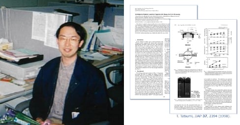
When Tatsumi was working for ASET / Left: at the office of ASET, Right: examples of published papers
By the end of the project, Tatsumi had taken on a leadership role. The experience he gained there would be put to good use in his research at Sony.
Through the project at ASET, I thoroughly researched the processing technology for fabricating the fine contact holes in the insulating film used to connect the wiring and transistors of semiconductor devices. I think my greatest achievement was to be able to comprehensively understand and model the process of dissociation and decomposition of fluorocarbon gas used in the processing of insulating films, how many particles are injected onto the substrate per second, and what is necessary to control this process. This is a technique that is still widely used in the development of state-of-the-art equipment and processes used in Japan and abroad.
This progress in understanding the technologies that underpin manufacturing has opened the way to the application of new materials used in new devices, which I have been able to apply to my research and development since returning to Sony. For example, my experience at ASET was hugely helpful during a collaboration to develop an LSI (Large-Scale Integration) called advanced CMOS (Complementary MOS).
90% of new technologies are found outside of the company.
Tatsumi also plays a major role in the exploration and promotion of plasma processing and other technologies not only within Sony but also outside of the company.
Currently, as a distinguished engineer of Sony Semiconductor Solutions, I am mainly responsible for the development of plasma process technology, support for device development projects, and human resources development. In addition to that, I was nominated for the position of Vice President of the Japan Society of Applied Physics from 2021 based on my involvement since my student days, and I am also involved in its management. The society has about 20,000 members and deals with a wide range of technologies including semiconductors and plasma. By interacting with various researchers and students, I have broadened my knowledge, and the personal connections I have made through these interactions have become a valuable asset.
Since 2019, I have also been teaching classes on plasma processes as a specially appointed professor at the Tokyo Institute of Technology as part of a joint research course conducted by Sony. Amid concerns about the declining population and declining number of students studying science, I would like to work on fostering talented students and, from my perspective as an engineer at Sony, convey how knowledge and technology in applied physics will lead to new devices and a better society in the future.
I believe that more than 90% of new technologies are found externally. Through my own experience, I hope to convey to young people that it is very important for engineers to go outside the company and learn about the wider world.
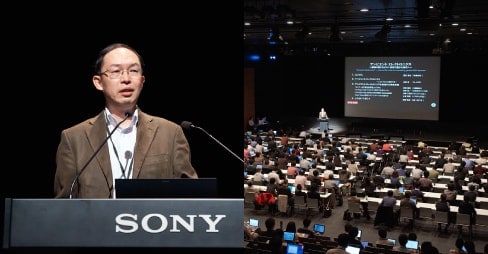
Left: Tatsumi gave a lecture to Sony’s engineers (2013)
Sony’s Engineers are “free” in many senses of the word
About Sony’s engineers, and what will be important for engineers in the future.
Engineers at Sony are “free” in many senses of the word. There are quite a few people in the company who can think outside of the box and create things that everyone else thinks are impossible. That’s probably the most amazing part. I believe that thinking outside of the box will be an even more important skill in the future. We live in an age where you can find any information with a quick search on the internet, but we should not be afraid of departing from conventional wisdom. In fact, we should take pleasure in it.
In recent years, the number of talented employees, as well as the general level of competency at the company, has risen. They have excellent application skills, work hard on highly specialized areas of development, and produce results within 2-3 years. If the young me of the past were to join the company today, I probably wouldn’t be able to keep up (laughs).
On the other hand, as may be the case with many companies, there are fewer and fewer opportunities for hands-on experiences in the research and development of manufacturing processes. Sophisticated modern manufacturing equipment automatically processes wafers at the push of a button, so what happens inside the equipment tends to remain a black box. In this age of convenience, I believe that one of my roles is to convey the importance of using imagination to quantitatively estimate the invisible reaction mechanisms.
People who can create a clear image of how technology will contribute to the world in the future will do well at Sony. It would be pleasuring that people with vision and a passion for changing the world with technology to join our company. So, I will do my best to create an environment where they will be free to devote themselves to development.


