Cutting Edge
Perspectives from the creators of the image sensor “microcosm”
Apr 10, 2019

In July 2018, Sony launched its IMX586 stacked CMOS image sensor for smartphones. The IMX586 has a small pixel size of 0.8μm (world’s first*) and 48 effective megapixels (the highest in the industry), for a higher image quality for an image pickup device. What kind of challenges and breakthroughs did the team encounter in the course of development? We invited the engineers in charge of pixel design, Image processing algorithm, and devices to tell us all about it.
*Among image sensors. According to Sony research. As of announcement on July 23, 2018
Profile
-

Masahiko Nakamizo
Mobile & Sensing Systems Division,
Sony Semiconductor Solutions Corporation -

Kazuhide Fujita
Mobile & Sensing Systems Division,
Sony Semiconductor Solutions Corporation -

Tomoyuki Watanabe
MIS Product Division,
Sony Semiconductor Manufacturing Corporation
Pixel design
Will the trend of miniaturization continue?
──First off, what is the role of pixels in an image sensor?
Masahiko Nakamizo:Pixels are the doorway from the visible real world to the electrical world—they convert the light coming through the lens into an electrical signal. Electrical signals converted by pixels go through analog and digital circuits and ultimately become images. This means that it is fundamentally difficult to remove noise that got in at the doorway—at the pixel stage—or to restore signal information that was lost at this stage. Thus, the foundation for making quality images starts with the signal from the pixels. If the pixels miss something, then an accurate image cannot be made.
──I see. So, what was the background for the development of the IMX586?
Nakamizo:Supposing that the sensor has the same surface area, the smaller the pixel, the more pixels can fit on an image sensor. The more pixels, the higher the image resolution. With smartphone cameras getting more and more sophisticated in recent years, every company has been striving to make pixels smaller to meet the demand for more advanced cameras that are still small enough to fit in a phone. So, in order to stay ahead of the competition, we needed to develop even smaller pixels.
With the IMX586, we were able to achieve a pixel size of 0.8 μm, which in turn made it possible to deliver a high resolution of 48 effective megapixels even on a compact sensor of 1/2 inch (8.0 mm diagonal).

──What was the smallest pixel size prior to your achievement of 0.8 μm?
Nakamizo:It was 0.9 μm, and before that it was 1.0 μm. Downsizing even 0.1 μm is, in fact, incredibly difficult. We anticipated that we would need to go smaller based on current trends, so we were able to start internal development prior to getting any specific requests from our customers. Then, once the decision was made to bring it to market, we accelerated our development. However, the trend of miniaturization is about to enter a turning point. That is, we will eventually reach the limit for simply making pixels smaller and face tradeoffs due to miniaturization.
The key to further performance improvement is overall optimization
──So, are there pros and cons to miniaturization?
Nakamizo:Yes. One of the drawbacks to miniaturization is that sensitivity declines. Of course, we try to develop it so that the sensitivity doesn’t decline, but we can see that it is time to try to create value in a direction other than that of pixel miniaturization. So, we are discussing various approaches for creating new value. These include, for example, incorporating sensing functions and leveraging not just high resolution but also the pixels and circuits to produce the most beautiful images overall. While collaborating with other teams, we are looking for new ways to improve performance by looking for the optimal ways to improve characteristics even more than before.
──Can you share any examples of how overall optimization helped you overcome the challenges that you encountered during the development of the IMX586?
Nakamizo:Whenever endeavoring to make a pixel smaller, we first make a prototype and evaluate it. Usually it is a straightforward process in which we reflect the evaluation results into our image design knowledge and design concept, and that is pretty much it. However, during this development, we took the time to hold many discussions with those in charge of signal processing, analog circuits, and digital circuits, to identify anticipated concerns and preliminarily investigate countermeasures to take.
In particular, the signal processing hardware specifications are decided in the early stages of design, and once the circuit is set, it cannot be changed, which means that in case any concerns arise we typically have to wait until the next generation of circuitry comes along. However, this time, we were able to have a full discussion of that issue during the prototype stage. In so doing, we were able to address fundamental issues in a timely fashion while we developed the product. As a result, we were able to create new value that wouldn’t have been possible solely with pixel design.
The performance of pixels is also greatly affected by how they are manufactured. So, we made it point to go to the plant and discuss things with the people there on a regular basis to get their feedback and gather information. Anytime we had a problem with the characteristics, we worked closely and tenaciously with the team at the plant to find out if it was due to the manufacturing recipe not being followed accurately or due to manufacturing equipment troubles or other causes. This kind of process is also an important aspect of the role of a pixel designer.
Imaging and sensing
──Image sensors are used quite a bit for smartphone cameras right now, but what other applications will there be for image sensors in the future?
Nakamizo:I expect that they will spread to various areas, such as factory automation (FA) and other manufacturing processes, security, and in-vehicle cameras. Meanwhile, there will also still be room to expand for smartphones, for example, to meet the trend toward multi-lens cameras.
The trend of incorporating the sensing function with the imaging function is spreading to cameras across various applications. In the field of FA and security, there is a need for a different kind of value—not the usual picture quality aesthetic of images for human consumption. For example, in a factory it is important to increase the frame rate and capture subjects moving at high speed without blurring. In such case, there is no need for the image to appear beautiful to the human eye. When measuring distances, certifying labels, or monitoring suspicious individuals, it is more important to detect the subject than to produce beautiful images.
When the purpose is sensing, we have to think about what kind of sensor characteristics are most suitable for the given purpose. We are working together with other teams, as well, to explore the potential of image sensors for sensing applications and deliver new value.

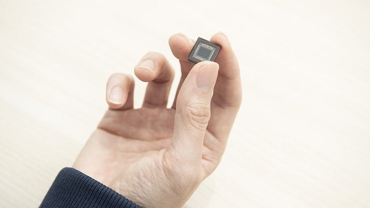
Test chip in development phase
──So, what is the strength of Sony’s image sensor?
Nakamizo:Personally, I think it is the difference in our pixel performance. Pixels are the doorway from the visible real world to the electrical world. This goes for both imaging and sensing. Everything starts with changing light to an electric signal at the pixel. This means we can differentiate our product by curtailing noise so as to realize high sensitivity performance and pioneering new pixel structures and miniaturization.
In addition, at Sony, we have people nearby thinking about signal processing algorithms, and we have the manufacturing company within our Group. This proximity gives us an advantage in that it makes it easier for us to find ways to achieve overall optimization. When issues arise, it is easy to gather the right people immediately to figure out the solution. Likewise, when we are trying to do something new, it is easy to find the people with the knowledge we need. Even when simply discussing new functions, it is easy to get the right people in one place, since we already know personally the people who are experts in each area. Once specifications are fairly solidified, then we can get the manufacturing team involved early on, and start discussing post-prototype testing and so on—all this keeps development moving along at a quick pace.
While increasing the speed of development like this, going forward, I also want our team to become even more capable of delivering new value.
In terms of sensing, our customers are still trying to figure things out about what they need. So, I think it will be critical for us to make proposals proactively to our customers. As we explore new fields for sensing, we need to approach customers like this: “With this solution using Sony sensors, we can provide you with more sensitivity and precision than you were imagining, and you can make use of those advantages in these other applications as well.”
Of course, as for the conventional imaging area, we want to leverage internal collaboration to deliver image quality that clearly differentiates Sony from all the rest.
Image processing algorithms
Image processing to deliver added value
──What role do image processing algorithms play in image sensors?
Kazuhide Fujita:Simply put, as the name suggests, our algorithms process the image. Specifically, we work on making the images clean and enabling new functions for the image sensor.
Specifically for the IMX586, our algorithms played a big role in functions such as the high dynamic range (HDR) image composition, the array conversion processing for the Quad Bayer color filter array that achieves both high sensitivity and high resolution, and the phase difference detection entailed in high-speed autofocusing. An example of our role is the solution we provided to accommodate the recent fad of portrait modes with soft-focus backgrounds.
──Could you tell us a bit more about the Quad Bayer array?
Fujita:When shooting a dark scene, such as a night scene, the signals from the four adjacent pixels with the same-colored filter are added together, making the pixel size equivalent to 1.6 μm (12 effective megapixels), thereby making it possible to shoot a brighter image with low noise. On the other hand, in the case of a bright scene, we use signal processing to convert the array into 48 effective megapixels in real time, enabling high-resolution shooting. That is what is meant by Quad Bayer array.

──What was the most difficult thing about the development of IMX 586?
Fujita:As pixels become smaller, the sensitivity inevitably declines. In other words, the quality of the resulting image will also decline or the noise will increase, hindering all the functions that we have already achieved, such as array conversion, HDR composition, and phase difference detection. So, that was the difficult part, trying to figure out a way to realize problem-free performance even when the sensor sensitivity drops a little.
Since miniaturization of pixels inevitably results in a decline in sensor characteristics, our role was to compensate through signal processing.
Also, since the high-speed autofocus function has become commonplace in modern smartphone cameras, users want autofocus regardless of the kind of array conversion being used or even when shooting in a wide dynamic range. In reality, however, it is very difficult to simultaneously perform array conversion and phase difference detection or HDR composition and phase difference detection that enables high-speed autofocus while compensating for characteristics. So, there were issues that could not be solved by signal processing alone. We needed to devise a driving method for signal readout from the pixels, and we were able to work with the pixel and other hardware designers to achieve overall optimization, which in turn enables us to make a breakthrough.
Still room for improvement in sensors for smartphones
──Now that the development of the IMX586 is over for the time being, what fields do you want to do more research and development in?
Fujita:In the last five to six years, the technology of stacking the signal processing chip under the image sensor has become pretty commonplace.
When it comes to image sensors for smartphones, there is a limit to the amount of surface area due to miniaturization. The most difficult and important point in further development is how to install as many functions as possible in a limited area. My basic aspiration is to improve the experience of users using smartphone cameras by delivering images on par with the beautiful images of interchangeable lens cameras with good performance.
──What kind of possibilities exist for image sensors for smartphones, and what kind of preparations are you making for those?
Fujita:We are working to prepare for further miniaturization and are continuing with research to realize various functions other than capturing images using sensors. For example, we are looking to create experiences other than imaging by making it possible to measure the distance to the subject. I am not yet able to tell you about this in detail because it is under development, but speaking from the conceptual level, for example, we want to make it possible to measure the surface condition of objects and three-dimensional shapes.

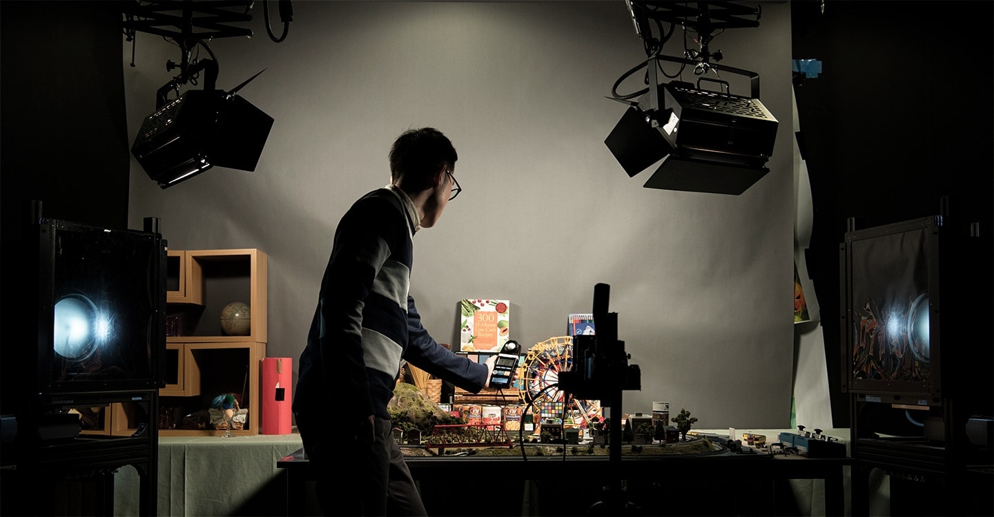
Image sensor evaluation environment
──What are the issues that must be solved for image sensors for smartphones going forward, and what fields other than smartphones, if any, do you think have potential?
Fujita:The challenge is to compensate for performance while maintaining the thinness of the smartphone. To maintain thinness, image sensors and lenses must be small. With this sensor, we were able to skillfully convert the array to compensate for the performance of smaller lenses and achieve electronic zooming comparable to optical zoom, but I think we will need to pursue further performance improvements in the future.
In fields other than smart phones, I think that there are various opportunities for image sensors such as automobile and monitoring applications. The social trend to use image sensors in all manner of areas will likely continue. I would like to integrate the technology we have amassed from developing image sensors for smartphones with other fields to find more ways to offer diverse kinds of value.
──What kind of career do you envision for yourself in the future?
Fujita:Going forward, the scope of sensing will expand, but in imaging as well, there are areas where development is difficult unless you know the characteristics of pixels and devices. If you understand pixels, devices, and signal processing, you are able to greatly expand what you can do. Originally, my major was closer to device design, so I am interested in device design. I think people who have cross-functional understanding of multiple areas will become more valuable.
I want to have the ability to devise solutions like, for example, “Well, to get these characteristics for this image sensor, we have to compromise this or that, and therefore, we will compensate with signal processing.” Using this kind of approach, I want to be able to achieve optimal solutions for the system overall.
Devices
The difficulty in balancing human resource development and technology development
──Please tell us about the role of Sony Semiconductor Manufacturing in designing, developing and manufacturing Sony semiconductors.
Tomoyuki Watanabe:There are two cases of development. One is when Sony Semiconductor Manufacturing takes the lead in device development, and the other case is that in which we work with Sony Semiconductor Solutions’ Device Development Department to perform joint development. The main role of Sony Semiconductor Manufacturing is to develop the manufacturing process and perform prototyping, improve characteristics and quality, and then implement mass production from that point.

──What role did you play in this development process?
Watanabe:Since joining the Nagasaki Technology Center, I have been in charge of developing image sensors for camcorders, monitoring, and smartphones, and large format sensors for digital interchangeable lens cameras. In 2016, when the Oita Technology Center joined Sony Semiconductor Manufacturing, I was transferred to Oita to join the startup team.
Working together with members from the Oita Technology Center who had joined Sony Semiconductor Manufacturing, we took on the challenge of developing the 0.8 μm pixel. During this time, I also provided other members with needed knowledge on developing and mass-producing image sensors, such as the process of development and the key points and know-how needed for development.
──What kind of hardships did you encounter in starting up this new product?
Watanabe:First of all, since the pixel size of the IMX586 was a world-first at 0.8 μm, the basic development started at Nagasaki, the core manufacturing site for smartphone image sensor development. However, due to circumstances related to other product development, resources and production, we decided to develop and produce in Oita.
The team at Oita was, frankly, very surprised with that move as we did not believe that we had enough experience in image sensor development compared with other Sony technology centers, and so we never thought that we would be at the forefront of product development for such a challenging technology.
Secondly, it had only been a little while since the Oita Technology Center joined Sony Semiconductor Manufacturing, so there were many differences in development procedure and culture. For that reason, it was my mission to find a way to smoothly integrate the culture of the Oita plant with the culture of Sony Semiconductor Manufacturing. In the development of IMX586, the schedule was very tight, so there were challenges with unifying all the team members while working at the same time to meet the timeline.
──When you look back, what is your take on the evolution of the image sensor?
Watanabe:When I joined the company in 2003, it was a turning point from CCD to CMOS image sensors. It was when the pixel size was 2 μm, so large compared to now, and image sensors for Hi-Vision were beginning to appear. Since then, the performance of image sensors for smartphones has dramatically improved, and with the increase in the number of pixels, it has become possible to take pictures of such quality that smartphones can fulfill the role of compact digital still cameras and camcorders. Miniaturization has progressed so dramatically, and it’s been impressive.
In the process of moving toward more pixels and greater miniaturization, Sony created a technical breakthrough—a back-illuminated structure. Conventionally, the wiring layer was placed on the light receiving surface and light was collected from the top, but by setting the light receiving surface to the top so that the wiring does not get in the way, we were able to greatly improve the sensitivity. With this technology, high-sensitivity capture is possible even with ultra-small pixel sizes.

Taking on the challenge of pixel depth control
──A moment ago, you mentioned the difficulties of developing in such a short period while also needing to help new members grow. What kind of difficulties were there in term of the actual manufacturing of the IMX586?
Watanabe:One process of manufacturing image sensors is photolithography. Simply put, this is the process of separating the areas that need to be processed from those that do not, as well as separating those areas that do need to be injected with impurities from those that do not, which is the most important step in building an image sensor. The smaller the pixel, the more it becomes necessary to build the photodiodes in the depth direction of the silicon substrate. To do that, you need to use greater energy to inject impurities into the silicon.
Also, in the photolithography process, we use a thing called thick film resist. This time it was particularly difficult to address fluctuations in the imaging characteristics due to the change in shape of this thick film resist. We had to spend a lot of time improving processing reproducibility using the same equipment and uniformity in the wafer surface.
──What role-sharing did you have with the development members at Kanagawa and Atsugi?
Watanabe:First, we starting consulting with the process engineers regarding the conditions for patterning in the photolithography process, which is the key point for pixel formation, to make sure that the patterning was following the pixel design.
After that, we did some prototyping to evaluate the results and improve the degree of perfection. Evaluations were performed by pixel designers from the viewpoint of imaging characteristics. A device team member in Atsugi checked the device characteristics, and a device team member in Oita checked the characteristics and process controls. So, in that way we were able to work together intensely to determine a process window that achieved the highest yield while meeting the required characteristics.
I think that being able to cooperate well by skillfully dividing the labor was one factor that helped increased the speed of this development.
──What is interesting about the development of the image sensor? What challenges did you face in the manufacturing process?
Watanabe:Sony is a great place that lets you interject your opinion into the development. Since Sony Semiconductor Manufacturing is Sony’s own plant, when I first joined I naturally assumed that it would be a relatively simple process of having the plant make the product according to Sony’s design. It turns out that it is never that simple, but it was very rewarding to be able to work with the Atsugi development team members in the field of device development.
I was really moved when an acquaintance outside work commented that the images from a video camera that had the first image sensor I worked on were beautiful. Getting that kind of reaction is the best part about working in manufacturing.
As for the challenges we face in the manufacturing process, they mostly consist of finding ways to keep variance to a minimum while maintaining a high yield. Since we do production across multiple plants to keep up with demand flexibly, we have to reduce the variance in imaging characteristics between plants to a minimum. We also must solve problems that occur due to differences of equipment and materials across plants, such as differences in characteristics and decline in yield.


