Cutting Edge
Sony’s Latest Image Sensors and the Technologies that Lies Behind Them
Oct 15, 2020

In the imaging and sensing field, Sony has a great selection of cutting-edge products, such as intelligent vision sensors with AI processing functionality, ToF image sensors that can be used even for AR/MR, and automotive image sensors critical to realizing autonomous driving. The unique technologies that lie behind these products are all world firsts, and include back-illuminated CMOS image sensors, stacked CMOS image sensors, and Cu-Cu direct bonding. We asked those involved to tell us more about these products and technologies and give us a peek into how they came to be developed.
<Topics>
1. Sony’s latest image sensors
1-1. Intelligent vision sensors
1-2. ToF image sensors
1-3. Automotive image sensors
Extra Feature: SWIR image sensors
2.The technologies behind Sony’s image sensors
2-1. Back-illuminated CMOS image sensors
2-2. Stacked CMOS image sensors
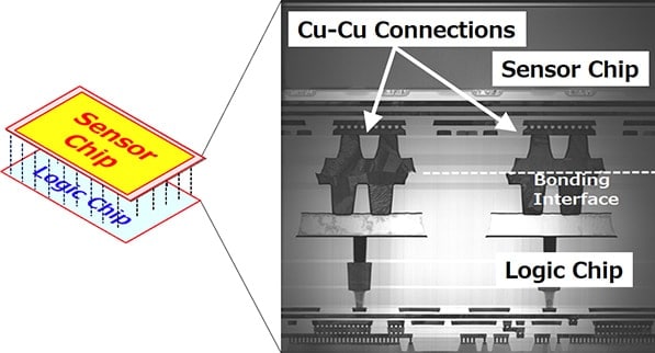
2-3. Cu-Cu direct bonding
1. Sony’s latest image sensors
1-1. Intelligent vision sensors
-

Ryoji Eki
SS Business Development Dept. 2
System Solutions Business Div.
Sony Semiconductor Solutions Corporation
──Please tell us a little about intelligent vision sensors.
Ryoji Eki:This is the world’s first* image sensor with AI processing functionality, and was announced in May 2020. It realizes high-speed edge AI processing. The pixel chip is back-illuminated, and the logic chip has a number of features in addition to the conventional image sensor operation circuit, such as Sony’s original DSP (Digital Signal Processor) and memory to store the AI model of users’ choice. This configuration allows a single image sensor to handle everything from image capturing to AI processing without high-performance processors and external memory.
* According to Sony’s research (at the time of announcement)

──What are their advantages and applications?
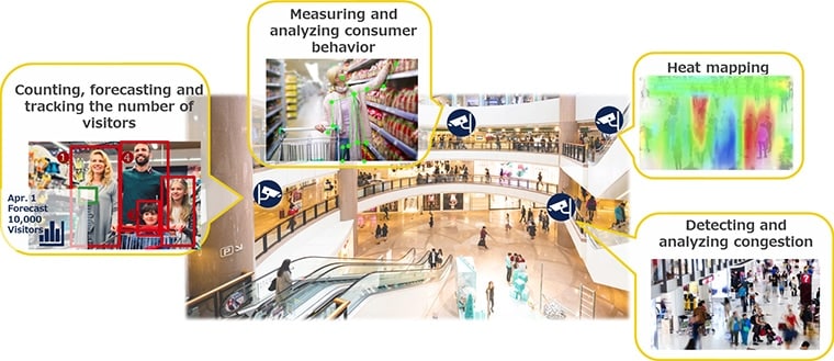
Eki:Extracting only the necessary data can reduce data transmission latency and power consumption of the camera and address privacy concerns when using cloud services. The reduced data usage of these image sensors will also help lower the power consumption of the cloud server. AI models can be rewritten and updated with the latest AI models to match various system environments and conditions. In addition to making the development of tiny cameras with AI functionality possible, these image sensors are expected to enable various applications in the retail and industrial equipment industries, and combined with cloud computing, will contribute to realizing optimal systems.
──What allowed Sony to develop the world’s first image sensors with AI processing functionality?
Eki:The biggest reason is that Sony already had the foundations of the development in place when we started planning. As well as expertise in developing system LSI, Sony had other necessary technologies such as back-illuminated CMOS image sensors, stacked CMOS image sensors, and Cu-Cu direct bonding that allow for high quality image capturing and multiple simultaneous functions. The core technology for processors specializing in AI was also being studied by a team from Sony Semiconductor Israel, and the original plan for the present DSP took form in 2017. However, there were few products that used AI at the time, and it was unclear what kinds of features were expected. Also, research into AI models progresses at a tremendous speed, so it is necessary to adopt AI processing specifications that will continue to be relevant several years following commercialization. We had to modify our original DSP plan over and over again before we were able to complete the intelligent image sensors.
1-2. ToF image sensors
-

Yohtaro Yasu
CV System Development Dept.
Mobile & Sensing Systems Business Div.
Sony Semiconductor Solutions Corporation
──Please tell us a little about ToF image sensors.
Yohtaro Yasu:With ToF (Time of Flight) image sensors, depth information is acquired by measuring the time it takes for an emitted light pulse to reflect and return to the sensor surface. There are various types of ToF, and we focused on developing an indirect-ToF (iToF) method that works by measuring the phase delay of returning light after it has been reflected by the target object. To realize this sensor, we developed a new back-illuminated CAPD*1 by combining CAPD technology, which is an IP of Sony Depthsensing Solutions, with Sony’s back-illuminated CMOS image sensor technology.
*1 CAPD: Current Assisted Photonic Demodulator

──What are the back-illuminated CAPD’s advantages and applications?
Yasu:Making the most of the back-illuminated structure, it efficiently converts light into electrons, enabling time detection of under 50 picoseconds and greatly improving distance resolution. It allows for miniaturization of 3D camera modules, and contributes to AR and VR through real-time acquisition of high-resolution 3D depth information. It is used for face recognition in smartphones, features related to AR and VR, and autonomous robots and drones.
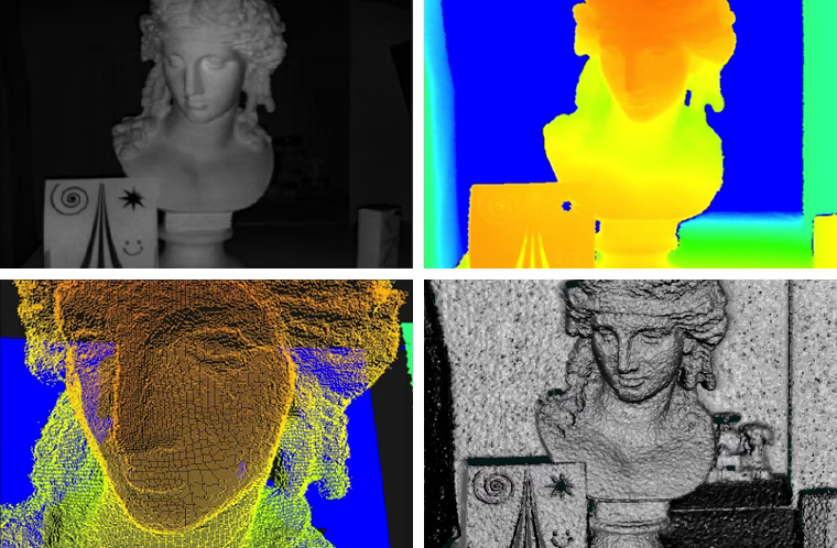
Clockwise from top left: (1) Monochrome output, (2) Depth Heat Map, (3) Point cloud display, (4) 3D display
──What was gained through the collaboration between Sony Depthsensing Solutions and Sony Semiconductor Solutions?
Yasu:Sony Depthsensing Solutions had been engaged in iToF R&D for many years and had a great deal of expertise. Development of back-illuminated CAPD uncovered synergies with Sony’s device and circuit technology. Sony Depthsensing Solutions was an emerging company at that time and only a small number of skillful members were involved in the development. Right after we started collaborating, the difference in corporate cultures perplexed us. By making Sony Semiconductor Solutions’ team small too, requiring each member to be more responsible, we were able to realize rapid development while absorbing this unfamiliar culture. During the development, issues that we had never experienced before cropped up, including chips breaking while under evaluation, but we worked with each other and brought them to completion. In addition to image sensors, this collaboration between the two companies from Belgium and Japan also contributed to securing the iToF businesses. We developed systems such as software that can generate smooth depth images, small module designs, and highly efficient laser drivers.
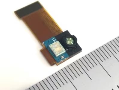
ToF camera module for smartphones (module with the IMX316)
1-3. Automotive image sensors
-

Noritaka Ikeda
Automotive Business Dept.
Automotive Business Div.
Sony Semiconductor Solutions Corporation
──Please tell us a little about automotive image sensors.
Noritaka Ikeda:These image sensors are used in sensing and viewing cameras for autonomous driving (AD) and advanced driver-assistance systems (ADAS). In addition to high resolution and high sensitivity, HDR (high dynamic range), LFM (LED flicker mitigation), and safety performance are also important.
Even in situations of dramatic lighting changes, such as when entering or exiting tunnels, they can capture high-quality images and flickering LED displays at the same time. The image sensors use technology that guarantees a long enough exposure to capture the LED while preventing pixel saturation caused by bright subjects, as well as unique pixel structures and exposure methods to achieve simultaneous HDR and LFM functions. Furthermore, our products meet the requirements of the AEC-Q100 automotive electronic component reliability tests. We also satisfy a design quality that is required for the functional safety requirements of automobiles, have introduced a development process that complies with ISO26262 automotive functional safety standards, and adhere to the functional safety requirement level ASIL for failure detection, notification, and control.
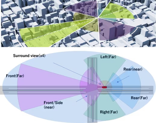
──Until recently, Sony was mainly handling image sensors for mobile devices and security cameras. What are the strengths of Sony’s automotive image sensors?
Ikeda:We at Sony have built up expertise at our production bases in Japan over many years and have managed to realize image sensors with high sensitivity and less noise. These key features can be extremely important for automotive image sensors, too. For example, since it is so hot inside and outside the car in summer, automotive image sensors need to operate in a wide range of temperature conditions. The upper limit is currently around 125℃. In general, the higher the temperature is, the more noise is generated by image sensors, but Sony’s image sensors are capable of capturing images with little noise even at high temperatures. They also have high sensitivity and are capable of picking up pedestrians in pitch darkness, who could not be seen with the driver’s naked eye, even with lights turned on. In addition, Sony’s stacked CMOS image sensor technology helps with further differentiation. They allow for image sensors with complicated and comparatively large-sized circuits, allowing for simultaneous HDR and LFM functionalities. In the future, we believe that by incorporating AI functionality into them, it will be possible to process a huge number of images taken while driving and transmit only the necessary data.
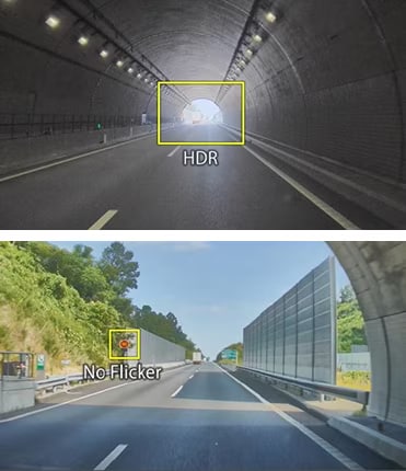
──What was difficult about entering the automotive industry?
Ikeda:What was toughest for us was dealing with the quality required to ensure safety. In the automotive industry, there are many international standards related to the product development process, which itself must also be refined along with the product in line with industry-wide standards. Using the evidence gathered during development, the validity of the process is demonstrated with the aim of establishing a firm position as a reliable supplier in the industry while being assessed and audited by customers. At first, we did not understand anything about the differences when compared with electronics products and the unique culture of the automotive industry, but we learned by reading standards and attending seminars, all the while striving to improve. In particular, it took a lot of time and effort to think about how to apply ideas defined on the vehicle level to the image sensor level. Image sensors will likely become more and more important for ensuring vehicle safety. We will redouble our efforts to develop our image sensors that contribute to the realization of a safe and secure society.
Extra Feature: SWIR image sensors
SWIR stands for "Short Wavelength Infra-Red." Instead of a conventional silicon (Si) based photodiode, a compound semiconductor indium gallium arsenide (InGaAs) based photodiode captures long wavelength light. However, since it is difficult to form an integrated circuit on a compound semiconductor, a separate Si layer is used for the circuit that reads the photodiode signals. A unique technology called "SenSWIR" connects these different semiconductors via a Cu-Cu direct bonding, realizing the Sony’s innovative SWIR image sensor. By thinning the indium phosphide (InP) substrate that blocks visible light, the SWIR image sensor is able to capture a broad range of wavelengths, from visible to short-wave infrared, with high sensitivity.
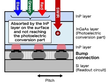
Bump connection
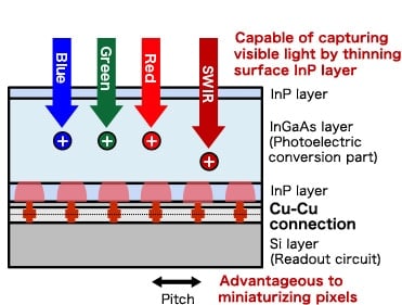
Cu-Cu direct bonding
Applications:
SWIR image sensors are used for material selection, contamination inspections, semiconductor inspections, and so on. In the pictures of the apples below, you can see surface information in visible light and subsurface information in the short-wavelength infrared light.
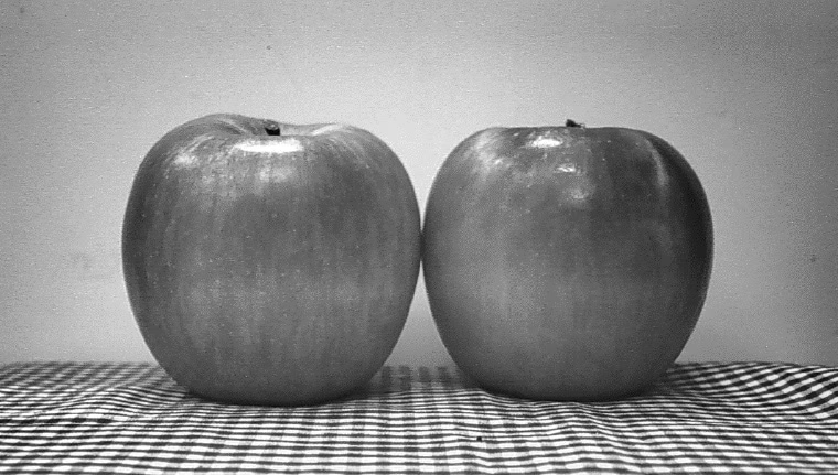
In visible light
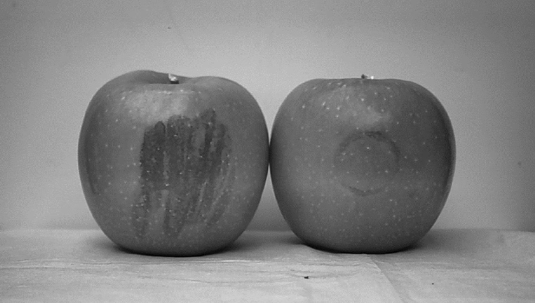
In the short-wavelength infrared light
2. The technologies behind Sony’s image sensors
2-1. Back-illuminated CMOS image sensors
-

Tetsuji Yamaguchi
Dept. 5, Research Div. 1
Sony Semiconductor Solutions Corporation
──Please tell us a little about back-illuminated CMOS image sensors.
Tetsuji Yamaguchi:This is a CMOS image sensor with a unique structure which differentiates the wiring layer and the light incident surface. In conventional front-illuminated CMOS image sensors, there is wiring that connects the various elements on the light incident surface. As such, the finer the pixels, the greater the reduction in sensitivity due to wiring blocking the light from reaching the photodiode substrate. To solve this, we developed substrate bonding technology to flip the photodiode substrate, high precision grinding technology to control the thickness of the substrate, and technology to suppress the noise during the grinding process. This allowed us to be the first in the world to commercialize a back-illuminated CMOS image sensor.
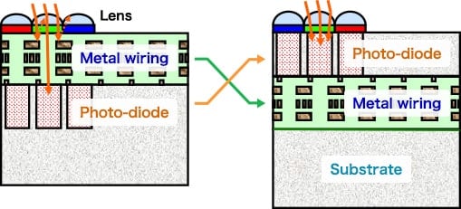
left: Front-illuminated structure / right: Back-illuminated structure
──What are their advantages and applications?
Yamaguchi:Higher sensitivity and better wiring layout improves image quality and allows for high speed recording. Finer pixels allow for the miniaturization of sensor chips, and by extension, miniaturization of products. It is used in digital still cameras, interchangeable-lens digital cameras, and smartphones. More recently, this structure has been adopted for ToF (Time of Flight) image sensors and has become the standard structure for CMOS image sensors.
──What is epoch-making about the development of the back-illuminated CMOS image sensors?
Yamaguchi:Around the time of development, based on the trend towards high-resolution image capturing and video shooting on cameras, CMOS image sensors that enabled lower power consumption and higher speed recording than CCD were expected to spread. Although a transition from CCD to CMOS image sensors was occurring for certain applications, the image quality of front-illuminated CMOS image sensors had room for improvement, and the transition itself brought up a number of issues. It is fair to say that developing the back-illuminated structure, which enables high image quality, accelerated the transition to CMOS image sensors. In the industry, the back-illuminated style was thought of as an ideal but difficult structure to realize from a technology standpoint. You might wonder why Sony was the first to develop it, but I think the key lies in the integration of technologies including the latest ones with those we had built up in CCD. For example, we adopted advanced processing technologies for the LSI we had nurtured in the gaming field when developing multiple processing technologies and device structures. The back-illuminated structure matches the stacking structure well and is capable of adapting to technological advancements. Combined with the growing trend of taking high quality photos on smartphones, it became incredibly popular. Now, over ten years have passed since its first commercialization, and it is still used for a wide variety of applications.

Front-illuminated structure

Back-illuminated structure
2-2. Stacked CMOS image sensors
-

Taku Umebayashi
Dept. 7, Research Div. 1
Sony Semiconductor Solutions Corporation
──Please tell us a little about stacked CMOS image sensors.
Taku Umebayashi:Instead of a supporting substrate that back-illuminated CMOS image sensors usually require to ensure mechanical strength, the stacked CMOS image sensor uses a circuit chip and has thousands of electronic connections between the pixel chip and the circuit chip. This world-first technology rearranges the pixel and circuit sections, which were previously placed on the same silicon chip, into two separate layers. Thanks to this structure, optimal manufacturing processes can be used for the separated pixel and circuit layers, while high capacity logic circuits can be fitted into a smaller area.

left: Conventional Back-illuminated CMOS image sensor / right: Newly-developed Stacked CMOS image sensor
──What is this technology used for?
Umebayashi:Due to its small size and high functionality, it was initially used in smartphone cameras for its ability to capture clear photos against strong backlight. Later, it became a platform technology for different types of sensors bringing about a variety of benefits including higher speed, lower power consumption, expanded functionality, lower costs, and improved productivity.

──What issues did you face during development?
Umebayashi:There were two major issues in planning the project. One was the question of how to stack the pixel section and the circuit section. As the goal of the development was to produce an image sensor that could be mass-produced for cameras on mobile devices, I concluded that wafer-on-wafer bonding technology was the only solution. Our technology was still in the early stages, but I was certain that this was the best among several methods. The other issue related to how best to make electronic connections between the pixel chip and the circuit chip on two different layers. I judged Cu-Cu direct bonding to be extremely difficult to control and decided to take the TSV (Through-Silicon Via) approach, which saw us putting holes in the silicon substrates and making connections using electrodes. In the back-illuminated structure, the pixel chip on the upper layer is thinned to be about 10 μm thick, a fifth of the usual thickness, following the wafer-on-wafer bonding process. This makes it possible to minimize the depth and the diameter of the contacts, shrinking them to about one five hundredth of their original size. This in turn allows for an overwhelming number of TSV connections. Later, we verified that it was necessary to make the circuit patterns on the lower layer ultra-flat prior to the wafer-on-wafer bonding, and it took about two years to succeed with the stacking. Creating a prototype meant a deadline was set, and insufficient processing margins led to a hard struggle. After we finally overcame these difficulties thanks to the hard work of the process development team, our project drew a lot of attention within the company and started progressing more smoothly toward commercialization.
2-3. Cu-Cu direct bonding
-

Yoshihisa Kagawa
Dept. 3, Research Div. 2
Sony Semiconductor Solutions Corporation
──Please tell us a little about Cu-Cu directing bonding
Yoshihisa Kagawa:This technology adds Cu-connection pads to the lower circuit chip and upper pixel chip of stacked CMOS image sensors to simultaneously establish physical and electrical connections. As the Cu-Cu direct bonding is made during the wafer production process, it requires an ultra-flat wafer surface and high precision wafer-bonding. Sony developed an original manufacturing process to overcome these issues and became the first in the world to roll out the technology.
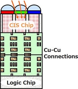
──What are the advantages and applications?
Kagawa:Miniaturizing the Cu-connection pads allows for smaller chip sizes and higher-density connections, simultaneously realizing greater productivity and functionality. As we can stack an incredibly large number of chips at once, it is faster and cheaper than the conventional manufacturing process for chip-level stacking. It is mainly used for stacked image sensors used in smartphones and contributes to miniaturization and greater functionality of chips.
──Why does Cu-Cu directing bonding make a difference?
Kagawa:With conventional stacking technology, TSVs (Through-Silicon Via), electrodes that vertically penetrate the semiconductor chip are used. They cannot be located in the pixel area because of this penetration and require dedicated spaces. In contrast, there is no penetration with Cu-Cu direct bonding, and therefore no such spaces are needed, allowing for much better performance than the TSV method as well as cost reductions. It was a difficult journey, but Sony became the first in the world to achieve mass production. In 2019, Sony received the 65th Okochi Memorial Production Prize for this from the Okochi Memorial Foundation. This technology is useful not just for image sensors, but also as a 3D-stacking technology for LSI in general. Development of higher functioning and higher performance 3D-LSI can be expected in the future.
